Tracing the Triad T2556
Part Three of a Series on the Triad T2556
Previously, I talked about getting all the muck removed. Now that the board is clean and doing something when power is applied, then next job is to figure out how everything connects together.
My first thought was that I could use a continuity tester to see how traces connected components. But there are a lot of traces, vias, and pins, and the act of having to flip the board over half a dozen times to follow each of the hundreds of paths would be a mammoth task.
I needed something better.
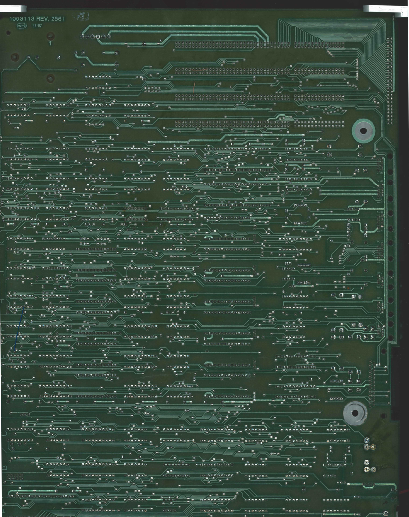 Scanned back side of the PCB
It turns out that trying to take a detailed and accurate picture of a 12“x15” surface is impossible with a cell phone.
Even if you have a tripod or something to keep the position of the camera stationary with respect to the subject, there are several problems with this approach. The lens has enough curvature that details at the edges are distorted, and furthest out traces are obscured by components that appear “in front” as well as “above” them. Without flat lighting, shadows also cause details to become obscured.
If only there were a device that could take a flat, linear picture of the board while shining light evenly and consistently over the surface.
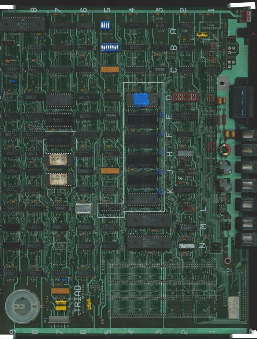 Scanned front side of the PCB
The good news is that a commercial grade photocopier does this really well! I 3D printed some corner pieces to lift the board slightly off the surface of the glass to reduce shadows, and scanned to email. The results appeared super clear, and were good enough to start.
 Posterized top side of the PCB
But the next question was how to overlay the top traces over the bottom traces?
I imported these two images into the GNU Image Manipulation Program (GIMP) and as I started work, it wasn’t long before I realized how big the images were.
So after wasting time for a while, I adjusted levels to give a great a contrast as possible, and then posterized the images to significantly reduce the number of colors. The net was that I could reduce each of the layers to 25% of the size of the original, which sped up processing time significantly. This also meant that I had more flexibility in adding additional informational layers later.
Unfortunately, the board wasn’t in exactly the same position when scanning each side because of flex in the board and the layers didn’t line up perfectly. It took some work rotating and distorting each layer using the Cage Transform tool until all the traces were aligned… or at least 50% of each via shared space between the top and bottom layers. Of course, the bottom layer had to be mirrored since to view this correctly since we will be effectively “looking through” the PCB.
In the end, I had a set of layers that I could switch on or off depending on what I wanted to accomplish. Some of these will be described in a little more detail below.
The devil, as always, is in the detail and it took a fair bit of effort to get things working the way I wanted.
Part of this was about making it as easy for my eye to process the information on the diagram as possible, so worked on maximizing contrast as I added working layers. Cognitive load, and all that.
The areas on these working layers have to be transparent, otherwise it wouldn’t be possible to see through that layer to the one below. At the bottom of the stack, I used a dark purple as the substrate color. This seemed to work better than a pure black.
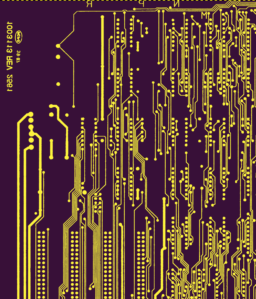 Resolved back side traces
If you look closely at the white circles which terminate traces on the posterized image above, you’ll see that a lot of them have a halo. On the left-hand side, you can see where the green vertical strip fades into the numbers. At the bottom of some of the components (like the 74S32 at grid reference N8), there is a shadow which has turned the green traces to gray. In spite of filtering, there was also a lot of noise left over in the image which caused distortion or speckling in the traces.
These artifacts and others meant that I had to go over each of the images trace-by-trace to make corrections.
It took a fair bit of work, but you can see how the back side traces ended up here.
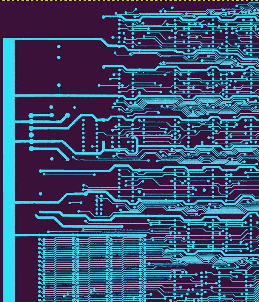 Resolved front side traces
The front side was harder though.
The easy bit was cleaning up using the same process as the reverse side, but then I realized this is not the complete picture: all of the traces on the top side of the board were obscured by the components!
I could refer back to the actual board and sneak the missing detail from below the axial components like resistors and capacitors, but all of those black dual-in-line packages made things super tricky by hiding a lot of information.
 Original front-side traces before mapping, showing obscured traces
It took a mix of intuition, flipping the board over a lot, and copious use of a continuity tester (along with a sprinkling of foul language) to figure out these missing traces and draw them in. The task was made slightly easier since I’d de-soldered the various damaged headers.
 Aligned top and bottom traces with silkscreen
I also knew that I’d want to reference the silkscreen markings at some point, so I separated these out into their own layer too. ProTip: GIMP has a ‘select by color’ feature, which made it easy to grab most of the silkscreen and paste it into its own layer. I say most… there was definitely some rough areas, but it’s good enough now.
One thing that I did later to improve the ability to read the silkscreen was to add a one pixel black outline. I did this by selecting everything in the layer, growing the selection by one pixel, and creating a new layer below the silkscreen where I filled that selection with black before merging the two layers. It worked pretty well.
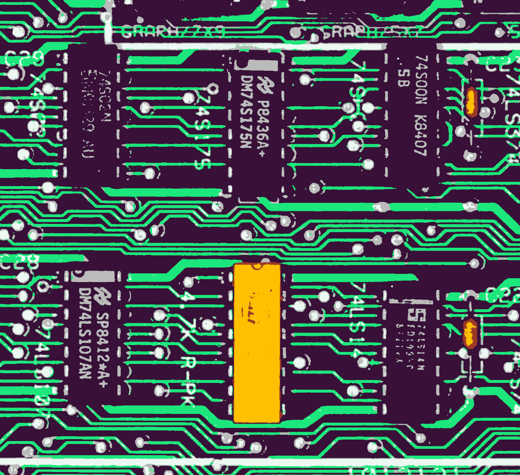
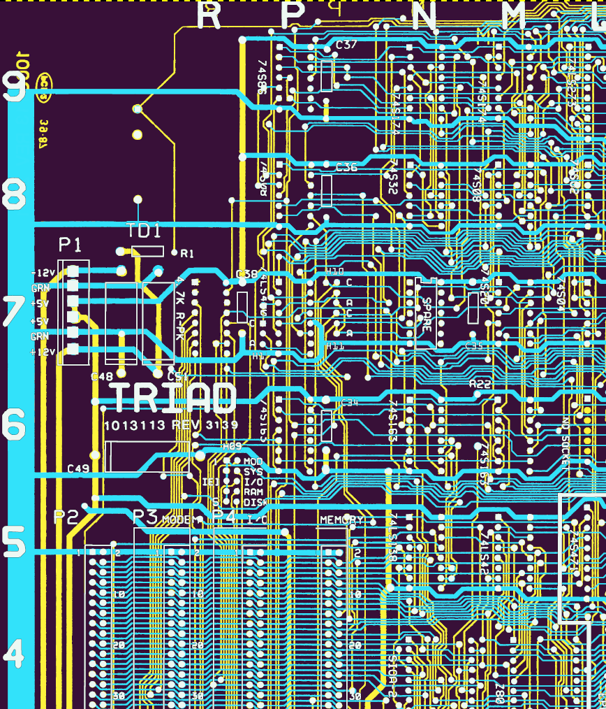 Aligned front, back, silkscreen, and thruholes
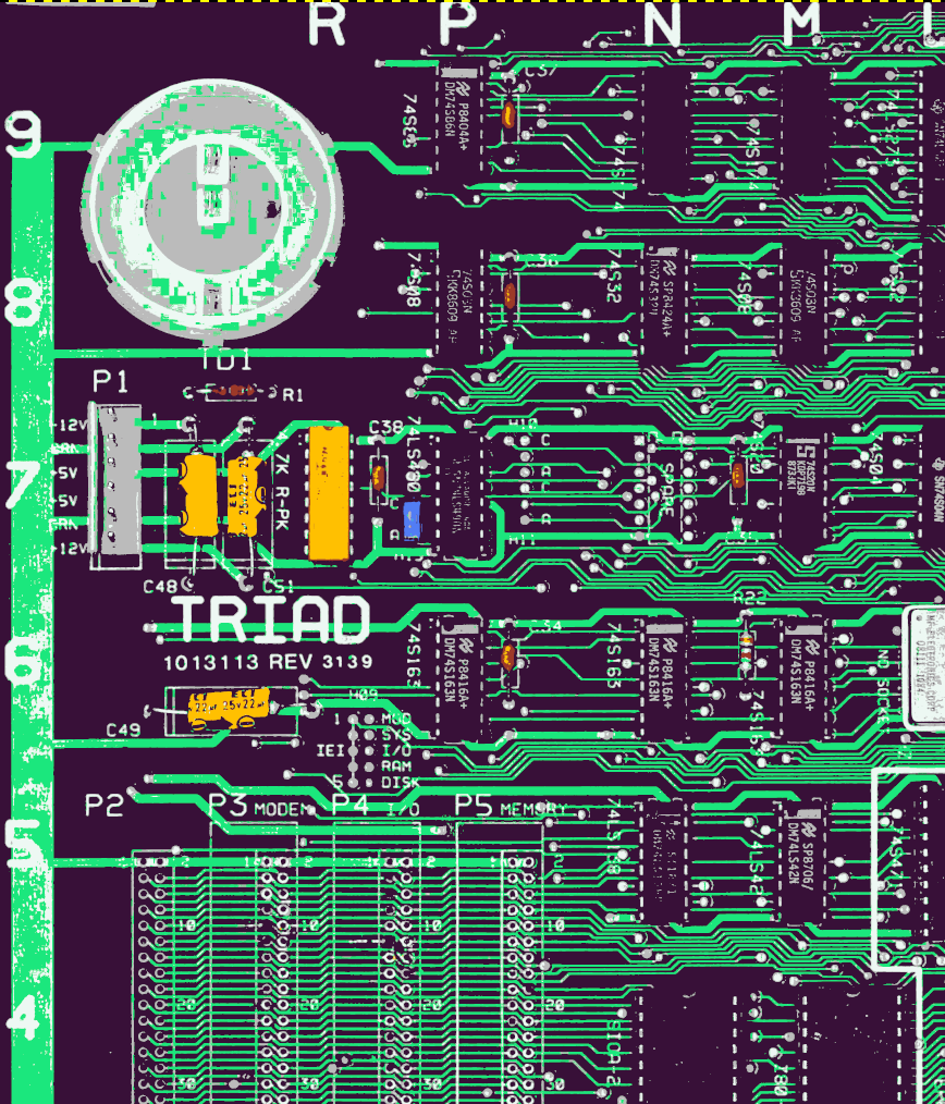
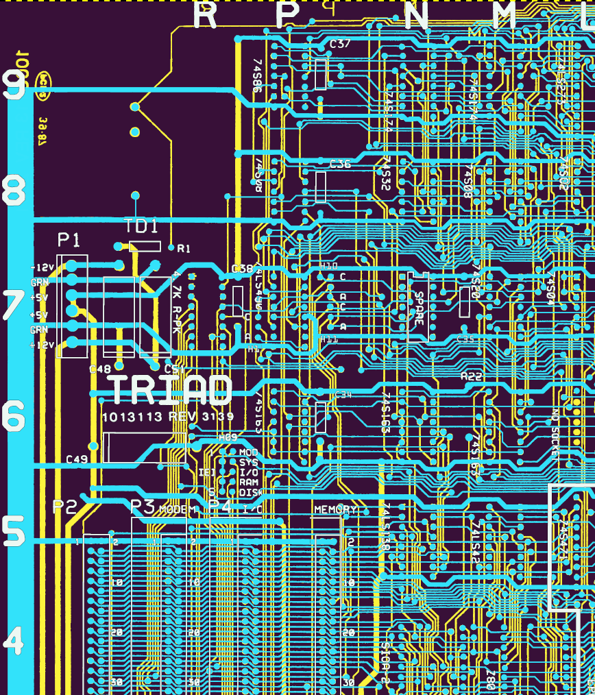
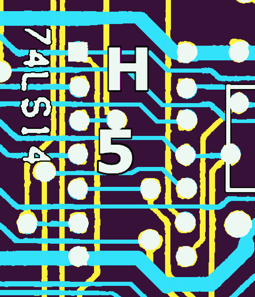 Map address example and trace detail
To aid in identification, and for another side project I was toying with at the time, I added a ‘Thruholes’ layer and applied a circle (square for pin 1) at each site using an appropriately shaped and sized brush.
When I later got into tracing pathways between devices, I started out by scrolling to an east-west and then north-south edge to get the map reference of the starting point, tracing through to the termination, then repeating the scrolling exercise to get the address of the end point.
You can imagine how much extra time this cost me. I wish that I’d added an Address layer much earlier in the process so that I could see the map reference of each and every integrated circuit on the board without having to scroll to the edge.
Here’s an example of the address text. You can see that I gave the address text the same outline treatment as the silkscreen, although it would have been better if I hadn’t anti-aliased the text: you can see the purple artifact on the letter ‘H’ that appeared as I modified the color map.
You can also see from this image that I had a ‘good enough’ threshold on cleaning up the traces, and the clean cyan lines that run horizontally are where I filled in the gaps below a component.
I lost track of the amount of time that this took, but it was clearly a horrific amount of effort. When I step back and see this, I still get a sense of satisfaction from the accomplishment. I’m okay with that.
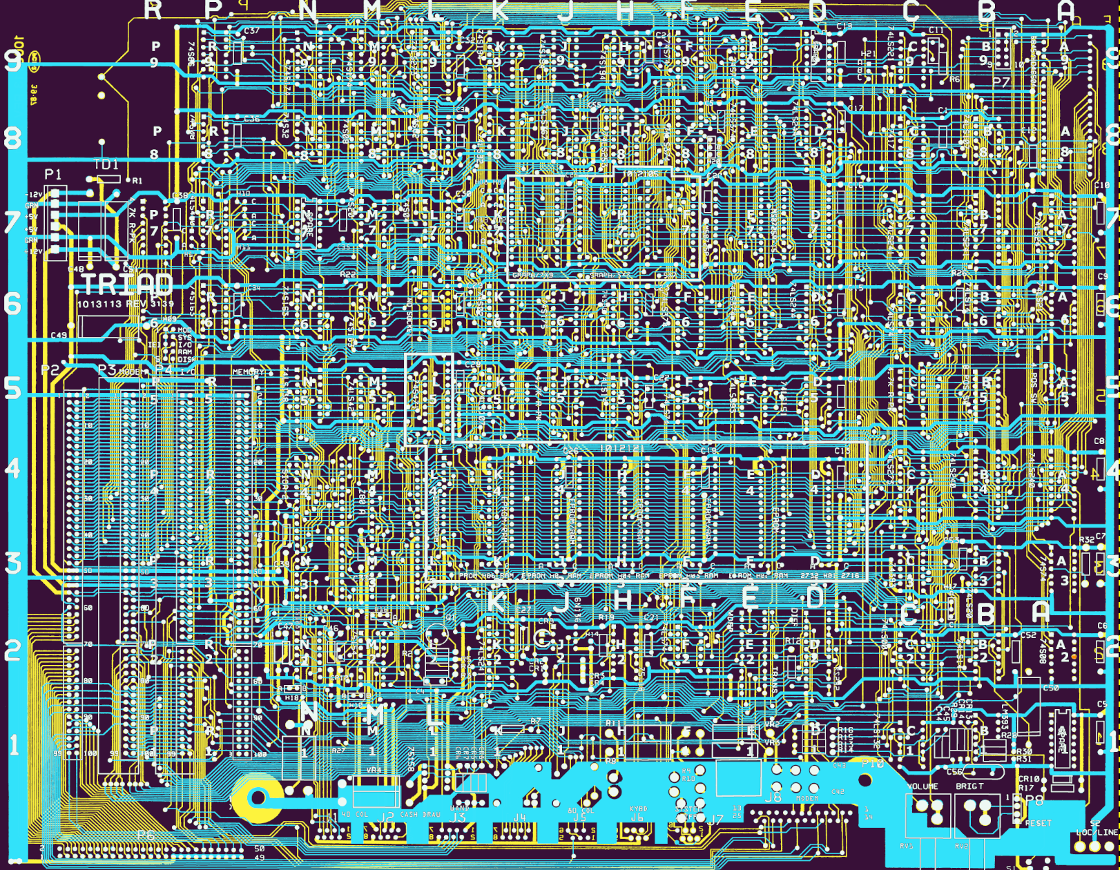 The Whole Enchilada
This doesn’t answer the spirit of the question that the article opened with, though: how does everything connect? For that, we’ll need to take these images and turn them in to a schematic.
That’s for another day though: first I needed a really, really, really long nap.
This article originally appeared on Medium.