Restoring the Triad T2556
Part Two of a Series on the Triad T2556
In the first part of this series, I realized that I had a lot of work ahead of me. The first step is to clean the case, wiring, PCB, and tube. Then there were some repairs to make.
 A startling contrast
The machine had spent years, or possibly decades sitting on a counter in an auto parts store, so it’s not surprising that it had picked up some dirt along the way.
In my youth, I would have thrown caution to the wind and blasted the board with a stream of hot water before leaving it somewhere warm with a lot of airflow to dry. But I’m older, and this board is one of a kind.
The first step, then, was to clean the PCB with isopropyl alcohol and a lot of cotton buds. I mean really, a lot of cotton buds. For some of the more awkward areas such as underneath the axial components and the ridges of various connectors, I used a toothbrush soaked with alcohol first, and then mopped up the area with cotton buds. This whole process took two or three passes, but the results were spectacular.
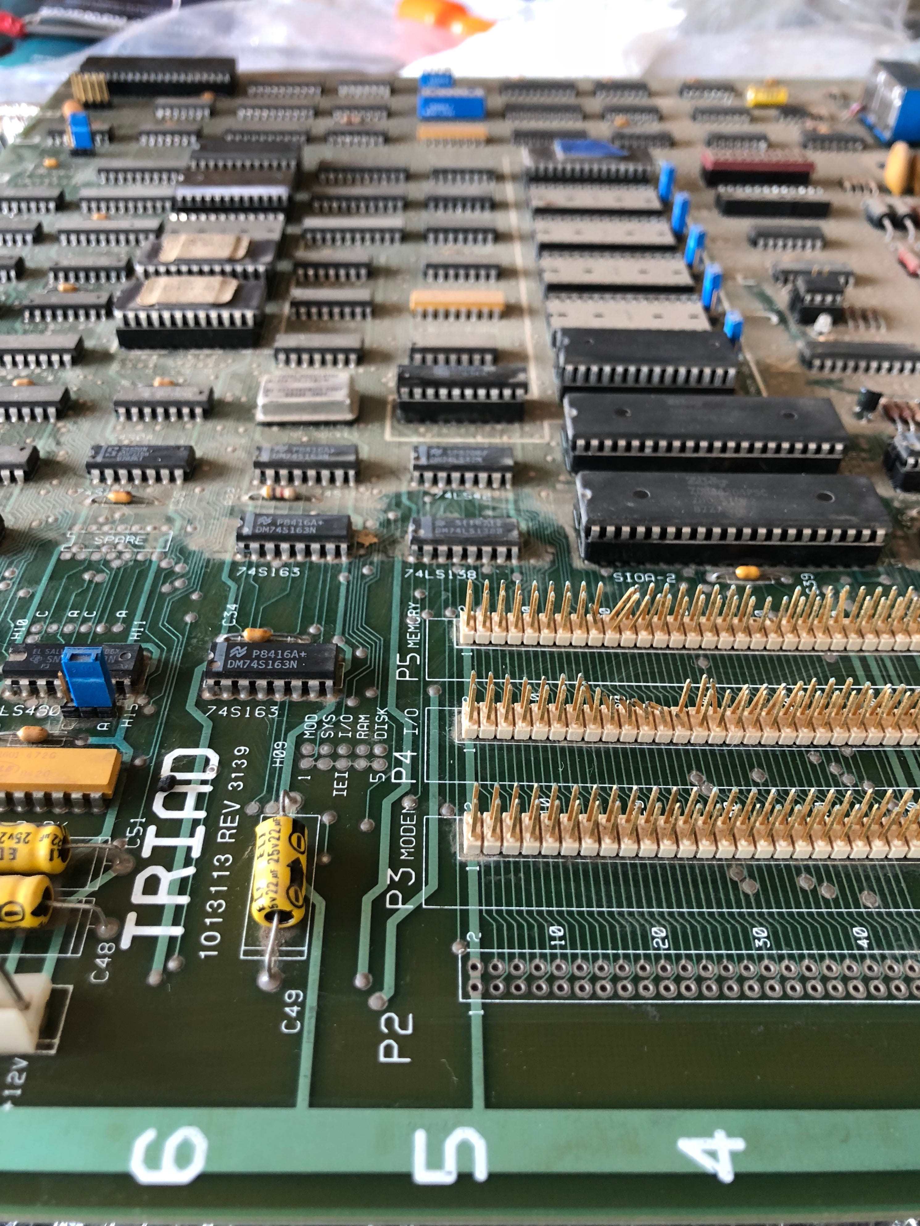
It became apparent as I was doing this that this truly is an old circuit board: excepting special cases, modern processes remove just enough copper to ensure that the traces (connections between components) are isolated, whereas here you can see that most of the copper has been removed. There is also what appears to be a ridiculous number of traces back and forth (on the top side of the board), and up and down (on the rear) all connected with a huge number of vias (holes which electrically connect a trace on one side of the board to the other). Probably the routing of connections between components was done by some automation, but that will be something to look at another time.
 Slowly but surely
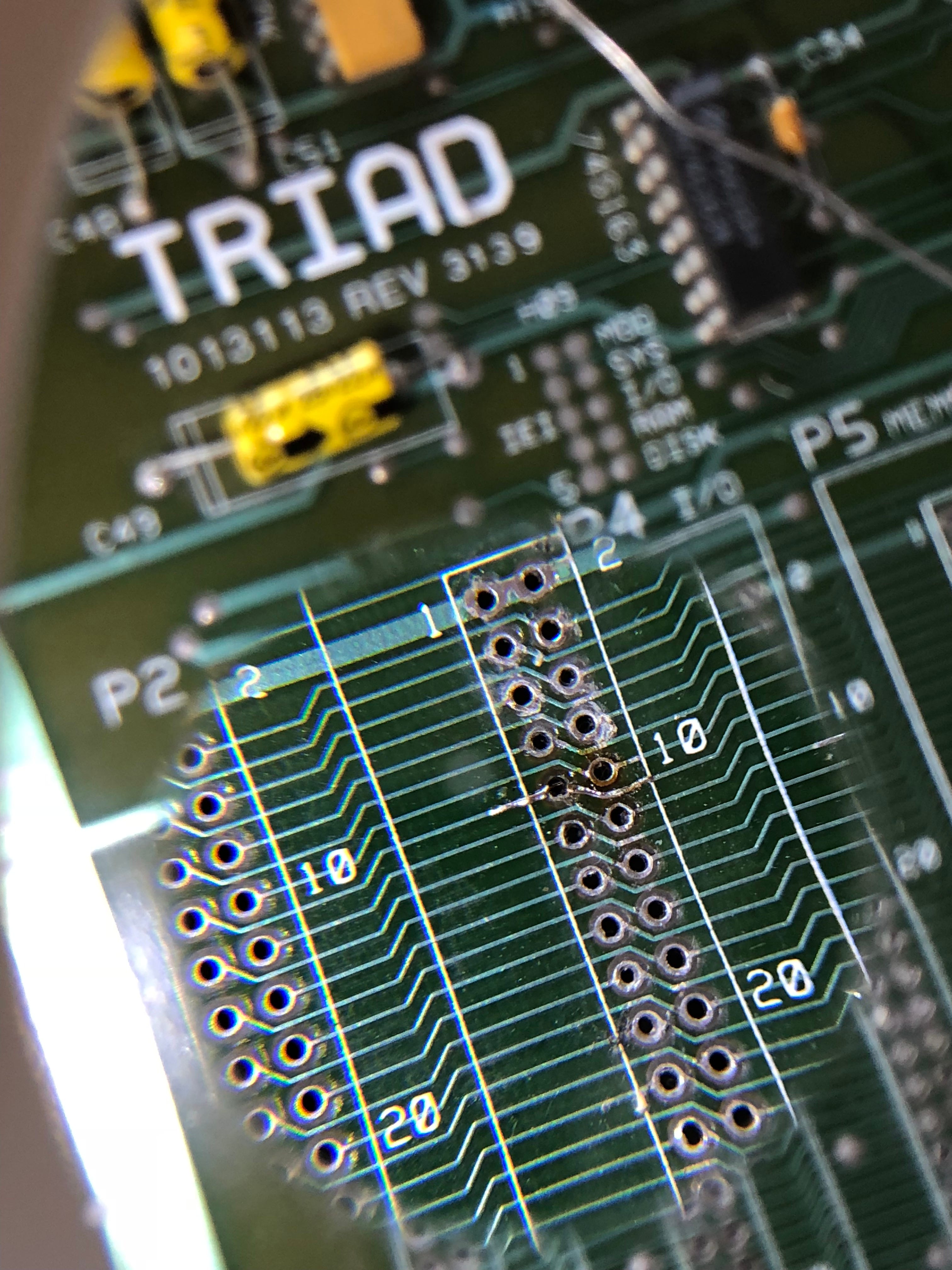
Now to removing those old connectors. You can see here that I tried to remove this 30-pin connector to start, and it was ridiculously hard work. It’s more or less impossible to melt all 30 solder joints at once with a soldering iron, especially when there is solder on each side of the board.
So I learned that I had to snip the plastic at the base of each pair of pins and remove them individually.
Whereas a reel of solder wick helped with the removal, there are several lessons I learned later that would have proven incredibly useful.
Running fresh solder over the joints earlier would make them easier to work with.
Perhaps if I’d invested in a solder re-work station for $50, I would have saved myself a few hours of pain and effort, since the hot air is better at gently distributing heat over an area.
There is a special solder alloy that has a much lower melting point than regular solder. Adding this to the joints may have made the whole process easier.
Using a solder flux pen may have helped too.
 Hooray!
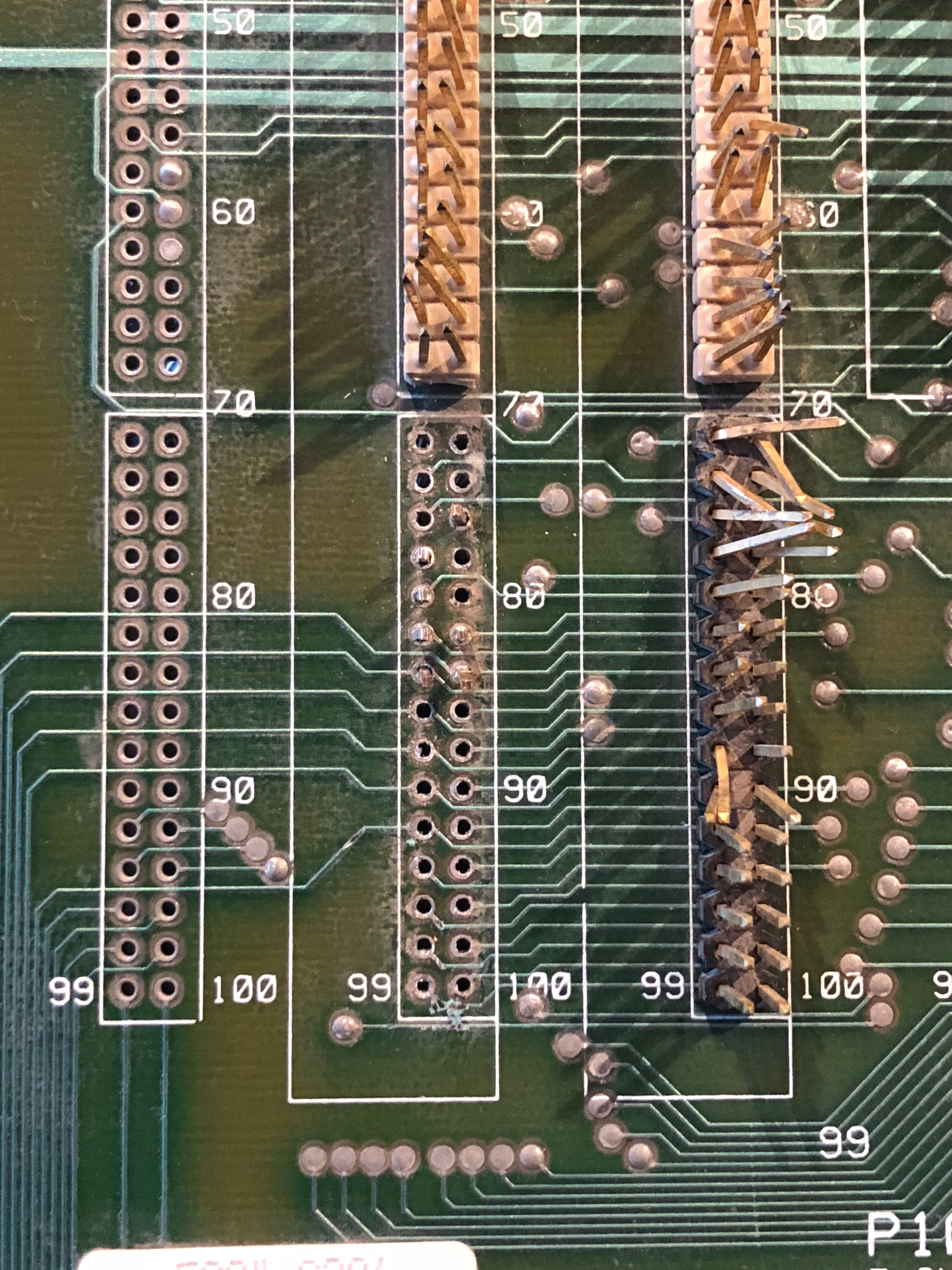
In the end though, the battle was won, and all the connectors gave way to whatever was underneath.
The brown splotchy areas you can see is residue from solder flux, and — although it’s common to see when you’ve just dumped a ton of solder on a board to convince parts to separate — it’s ugly and pretty clear that I hadn’t done anything like this in a long time. Possibly ever.
Fortunately, it can be removed by a gentle scrub with a mix of isopropyl alcohol and acetone and then some mopping up. This was a good lesson to learn, and I always have a bottle of acetone close by now.
 Ooops.
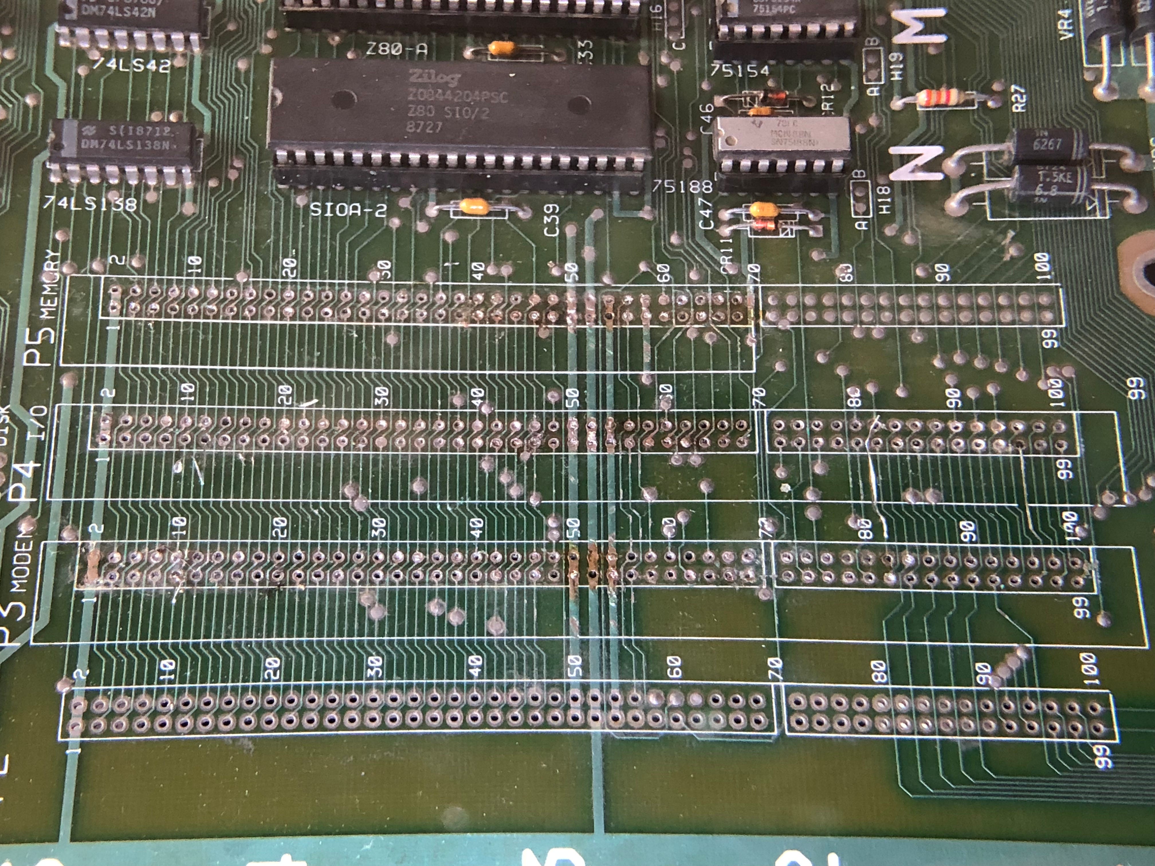
Unfortunately, it wasn’t all good news.
There were areas where I used too much force or too much heat, and the copper traces lifted from the circuit board.
Not good.
It was possible to fix some of these by super gluing down the loose tracks, and running fine threads of wire across the gap to restore missing traces, but not all. In some cases, the damage was too severe and I had to bridge using bodge wires on the back of the PCB.
This permanent damage is by far the most frustrating part of the project, and incredibly regrettable. At least I have a list of things I’ll do differently if I decide to do something like this again.
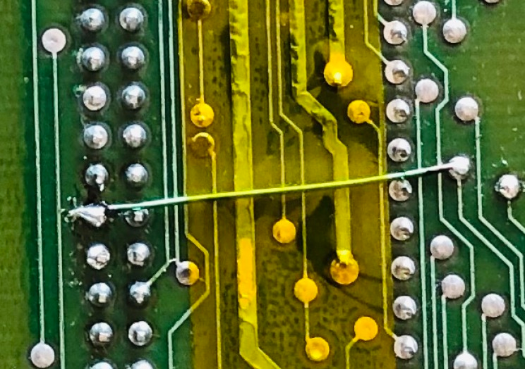 A bodge wire on the underside of the PCB, protected with kapton tape
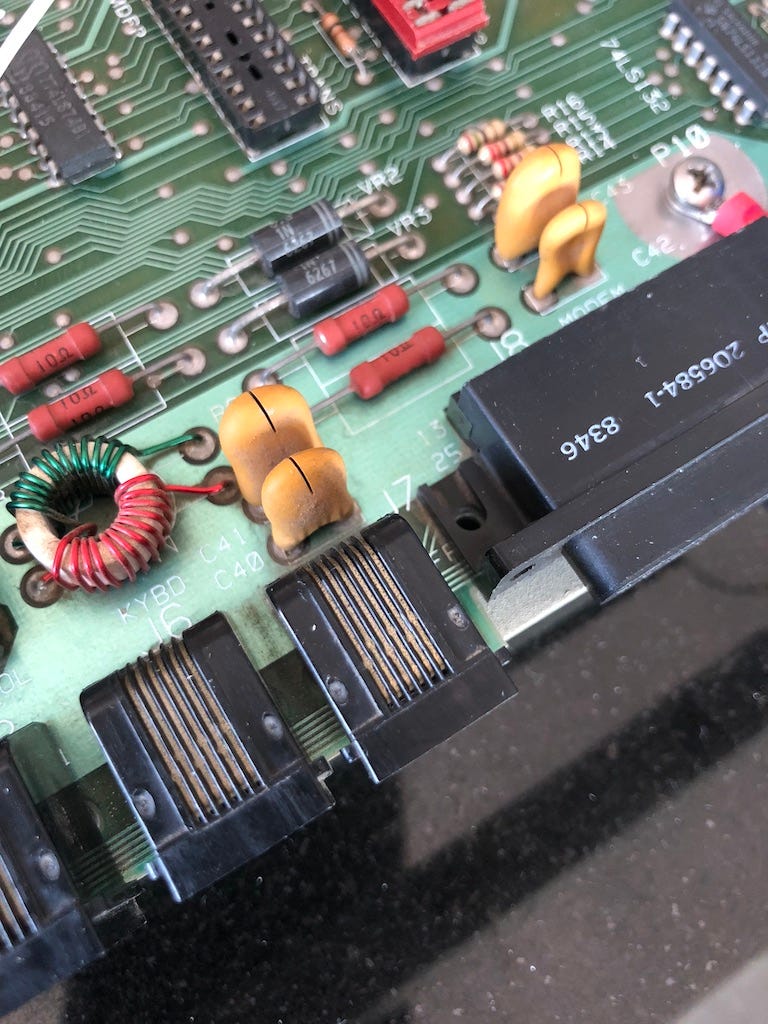
The rest of the cleanup was straight forward: for insulation and plastic, I used warm water with dish soap carefully applied, again the toothbrush came in handy for difficult corners.
The only other cleaning part that proved challenging was the cream-colored case. Dish soap and water took off some of the dirt, alcohol a little more, and acetone did nothing (I was also worried that acetone would melt the case, but it turns out that the cream color is some sort of hard wearing enamel paint.
In the end, the only thing that made a substantial difference was to rub the surface lightly with baking soda. Perhaps the abrasive in Barkeeper’s Friend would work just as well?
Next, I checked the electrolytic capacitors on the main board, power supply and tube driver. These tend to decay over time and eventually pop, but all of them looked okay. This was a good quality product designed to last. Probably it’ll be a nasty surprise for me at some point, but I’ll worry about that when it happens.
I still had the mounting brackets to repair, and the potentiometers to replace, but my patience was wearing thin. I wanted to plug the PCB back in to the power supply and see what would happen.
The outcome was a series of R2-D2 style beeps, followed by a continuous beep-boop alarm sound. What did it mean? Is it good?
The only way I would find out is by learning more about the hardware. But that’s for another day.
This article originally appeared on Medium.